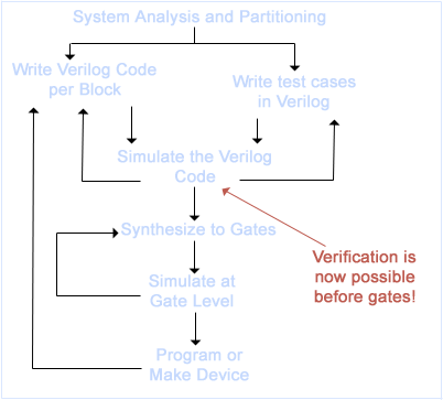
The diagram below summarises the high level design flow for an ASIC (ie. gate array, standard cell) or FPGA. In a practical design situation, each step described in the following sections may be split into several smaller steps, and parts of the design flow will be iterated as errors are uncovered.
System-level verification
As a first step, Verilog may be used to model and simulate aspects of the complete system containing one or more ASICs or FPGAs. This may be a fully functional description of the system allowing the specification to be validated prior to commencing detailed design. Alternatively, this may be a partial description that abstracts certain properties of the system, such as a performance model to detect system performance bottlenecks.
Verilog is not ideally suited to system-level modelling. This is one motivation for SystemVerilog, which enhances Verilog in this area.
RTL design and testbench creation
Once the overall system architecture and partitioning is stable, the detailed design of each ASIC or FPGA can commence. This starts by capturing the design in Verilog at the register transfer level, and capturing a set of test cases in Verilog. These two tasks are complementary, and are sometimes performed by different design teams in isolation to ensure that the specification is correctly interpreted. The RTL Verilog should be synthesizable if automatic logic synthesis is to be used. Test case generation is a major task that requires a disciplined approach and much engineering ingenuity: The quality of the final ASIC or FPGA depends on the coverage of these test cases.
For today's large, complex designs, verification can be a real bottleneck. This provides another motivation for SystemVerilog - it has features for expediting testbench development. See the SystemVerilog section of Knowhow for more details.
RTL verification
The RTL Verilog is then simulated to validate the functionality against the specification. RTL simulation is usually one or two orders of magnitude faster than gate level simulation, and experience has shown that this speed-up is best exploited by doing more simulation, not spending less time on simulation.
In practice it is common to spend 70-80% of the design cycle writing and simulating Verilog at and above the register transfer level, and 20-30% of the time synthesizing and verifying the gates.
Look-ahead synthesis
Although some exploratory synthesis will be done early on in the design process, to provide accurate speed and area data to aid in the evaluation of architectural decisions and to check the engineer's understanding of how the Verilog will be synthesized, the main synthesis production run is deferred until functional simulation is complete. It is pointless to invest a lot of time and effort in synthesis until the functionality of the design is validated.
Prev Next