In this article we're going to devote some space to a very neat little circuit that not enough designers know about.
The Problem
Synchronising from a slower clock domain into a faster one is an easy thing to do, and most designers are familiar with the common two- or three-stage shift register that accomplishes this for a single signal. However, passing information from a faster clock to a slower one is a different matter. How can this be done? The subject came up during a VHDL course at a well-known physics research establishment, where an engineer wanted to capture very fast pulses from a sensor. These pulses were very much shorter than his system clock period, but the maximum pulse rate would be quite a lot slower than the system clock. How could he reliably provide a synchronous pulse count to the rest of the system?
The solution
The answer lies in a circuit invented a few years ago by Rob Weinstein, (then with Memec) and christened the "flancter" by his colleague Mark Long. Rob's application note described a circuit that allowed a status flag to be set in one clock domain and cleared in another, and this is a useful thing to be able to do. Rob's note describes interfacing FPGA logic with a processor, each running with its own clock.
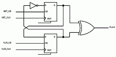
Let's have a look at the basic flancter first of all. It consists of a twisted ring of two flipflops with their outputs xor'ed.

When set_clk is triggered the output flag goes high and when clr_clk is triggered the flag goes low. So far, so good. There is one particular issue with the flancter that all applications must work with: operating the set and reset flip-flops must be mutually exclusive in time. That is to say, once the set_clk has been triggered and the flag set, it must not be triggered again until the flag has been cleared. Similarly, once the flag is cleared by clr_clk, it must not be cleared again until it has been set. Establishing this kind of interlocked protocol is the main task facing anyone wanting to use a flancter.
The Application
How can we use it to count our rapid pulses? We will use the flancter to detect the pulses and some other logic to count them. But there is something else to think about: the pulse-detect flag is asserted whenever an event arrives, and that is most certainly not synchronous with the sysclk. Hence we have some exta work to do, so synchronise the detect flag into the system clock domain before using it. In general, the output from a flancter must be synchronised into any clock domain that uses it, which may mean both the domain that sets the flag and the domain that clears it.
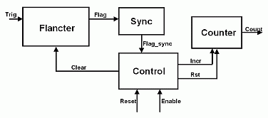
So what does our design look like overall? Here’s the block diagram:

A little explanation, as the diagram makes the design look more complicated than it really is. The counter, synchroniser and control blocks are pretty simple and are in fact a little dull:
- Counter has clock enable and synchronous reset.
- Sync block has two-stage synchroniser with synchronous reset.
- Control has just two states: wait_flag and flag_set.
All these are clocked by the system clock.
The flancter is the interesting bit, and needs more care in understanding (it needs more care in physical implementation, too, but we'll get to that in a moment). The trig input clocks the set_clk flop. When this occurs and the flag has been synchronised, the control block
- removes set_ce
- increments the counter
- asserts clr_ce for one sysclk
- asserts set_ce and clears clr_ce
In this application the clr_clk of the generic flancter is the system clock. We’d really like to keep the number of clock domains down, and with this arrangement we have just one special clock domain with just one flop in it. That is the trig input and the set flop.
Implementation
Here's where we get to the implementation considerations. Trig is a clock, and must be treated as such. Most FPGA tools will automatically identify it as a clock and route it through a global clock buffer, but this might not be correct for you. How many "proper" clock domains do you have? Is that at or close to the number of global clock resources available in your device? You have to know the answers to these questions.
Conclusion
What we have presented here is a counter for short-duration asynchronous events. The counter requires that events are seperated by at least 6 system clock cycles. The events themselves must be detectable by a flipflop in the target device; check your data sheets for the minimum 'high' width requirement for a flipflop clock pin. A quick scan of a few FPGA data sheets indicates that a minimum pulse width of a nanosecond or so is not wildly inaccurate.
The flancter should be in every designer's toolbox of useful circuits, and we hope we've shown why.
Downloads
Click here to download VHDL and/or Verilog source code for this example and this page in PDF format. As a service to engineers (and because it's become hard to find on the web) we are also hosting the original Memec Designs application note describing the flancter. All credit is duly given to inventors and copyright holders but if anybody has a problem with us providing this appnote then please get in touch. Rob, if you're out there...
In exchange for these downloads, we will ask you to enter some personal details. To read about how we use your details, click here. On the registration form you will be asked whether you want us to send you further information concerning other Doulos products and services in the subject area concerned.


