Standard Level - Live Instructor-Led Training
5 sessions (Live Online) 4 hours per session
PLEASE NOTE:
Important: You will find your overall experience and learning outcomes are much improved on this course by having active 2-way dialog with the course instructor, as well as interaction with other attendees. In that respect we highly recommend that you make provision for enabled webcams when attending.
Overview
This highly practical course is designed to take the student through the entire process involved in designing and fabricating high-speed PCBs. It begins with the fundamentals of electromagnetic fields and the behavior of transmission lines that are the basis for all high-speed signaling. From there, it examines all the aspects of high-speed design leading to the development of a robust set of PCB design rules that accounts for power subsystem design, routing rules, and design of PCB stack-ups as well as the fabrication rules needed to balance performance against cost and manufacturability.
The materials and examples used in this course are drawn from actual designs of high-speed systems in current manufacture. These examples range from video games to terabit routers and cover the complete range of designs. The design process presented is based on many years of completing designs that are “right the first time”. Attendees are shown many ways to improve their design process so that designs meet this objective. Reliable methods for controlling and containing EMI will also be thoroughly covered.
This course places special emphasis on very high-speed differential signaling protocols such as XAUI, HyperTransport, PCI Express, InfiniBand, SATA, SSCSI, Ethernet, USB, HDMI, and others that are the backbone of modern computing. Actual circuits are built and tested and then modeled to correlate modeling techniques. The topic of how to design power delivery systems capable of supporting these protocols is also addressed.
The course draws substantially from this real-time experience with state-of-the-art components, fabricators, and materials. It also draws heavily on the design of backplanes and daughter boards containing thousands of 2.4, 4.8, and 9.6 GB/S signal paths as well as some special cases with data paths exceeding 56 Gb/S.
This course is important to engineers and designers who are being asked to design PCBs and systems that have data channels operating above 1 Gb/S. to as high as 56 Gb/S.
It describes how to handle multiple (sometimes as many as 29) high current, low voltage power supplies present in these new products.
It also covers in detail how to design the transmission lines required by these signals in such a way that they have the bandwidth and low skew required for stable operation.
This course is also of value to new engineers and designers who are looking for a comprehensive introduction to high-speed system design.
|
· Design engineers
· System architects
· EMC specialists
· Signal integrity engineers
· Technicians
· PCB layout professionals
|
· Applications engineers
· IC designers
· IC package designers
· Test engineers
· PCB Fabricators
· Design & Engineering managers
|
- Attendees must have a good working knowledge of digital hardware design
- No previous knowledge of signal integrity or simulation tools is required
- No advanced math is required
Electronic designs of all kinds are operating with increasingly faster clock rates and rise times. At the same time, the pressure to complete designs in fewer design cycles is putting pressure on design teams to deliver designs to manufacturing that are “right the first time”. To account for the normal variations in component edge rates, propagation delay variations, amplifier gains, logic levels, and variations in the PCB fabrication process, it is necessary to invoke the use of design tools and methods that allow “preroute” analysis to ensure the final product is designed correctly. With the speeds of signals and components rising into the multi-gigahertz range, relying on the traditional breadboarding or hardware prototyping process often results in a product never making it to market.
This increase in component speed has made it necessary for all design engineers to master the design techniques that were once only the province of supercomputer engineers. This course relies heavily on the proven methods developed for supercomputers and terabit routers. It also draws on experience with disc drives and high-performance video games.
Problems Addressed in This Course:
- Failures from crosstalk and reflections
- Problems related to time delays in PCB traces
- EMI failures
- Failures stemming from poor power system design
- Failures related to poor IC package design
- Losses in the data paths
- Materials induced failures
- Managing very high data rate differential pairs
The course includes:
- An electronic copy of the class slides in color PDF format
- More than 120 articles and technical publications will be provided electronically to serve as a library for further reading
Session 1
- Review Transmission Line Fundamentals
- Type of transmission lines
- Calculating Impedance
- Terminations
- PCB Structures—right-angle bends, vias, plane cuts
- Cross talk
Session 2
- Differential Signaling
- IC Package Effects
- Power Delivery System Design
- What do Loads Look Like
- Deciding on a PDS Impedance
- Characteristics of Capacitors and Inductors
Session 3
- Power Delivery System Design Continued
- Determining How Many Capacitors are needed.
- Designing in Power Plane Capacitance
- Measuring the PDS Impedance
- Determining when a PDS Meets its Target
- Invalid Rules of Thumb about PDS Design
- Design Rule Creation Using Noise Margin Analysis
Session 4
- PCB Design Process
- Designing the PCB Stackup
- EMI Containment
- Developing a Set of Routing Rules
- Testing Fabricated PCBS
- Getting to 56 Gb/S
- Signal degradation sources- a real data path will be modeled as signal speed increases
- Bandwidth requirements for differential pairs
- How skew affects differential pairs
- How laminate choices affect skew
- Managing skew in differential pairs
- How laminate choice affects loss
- How the choice of copper finish affects loss
- How processing at fabricators affects loss
- Laminates currently available with which to fabricate high-speed PCBs
- Routing differential pairs for optimum performance
- Choosing connectors for high-speed differential pairs
- Connector pinout to minimize unwanted crosstalk
- How vias can affect signal quality
- When can vias be ignored?
- How to prevent vias from degrading signal quality
- Choosing materials that enable good signal quality without over-specifying
- Is a low DK (dielectric constant) material necessary for high-speed signaling?
- Handling high-speed differential signals on twisted pairs
- Handling high-speed differential pairs on flexible circuits
- Characteristics of new laminates developed for high-speed signaling
- Adaptive transceivers
- Equalizing techniques
- Simulation of high-speed data paths
- Documentation required to insure boards containing high-speed differential pairs are properly fabricated
Session-5
- PCB Fabrication
- Determining PCB Pad Stacks
- Blind and Buried Vias
- Summary
- References
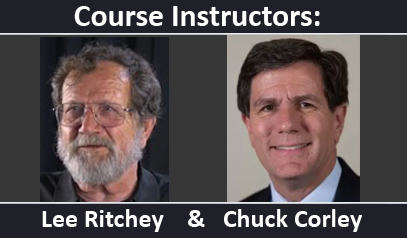
Lee Ritchey is one of the industry´s premier authorities on high-speed PCB and system design. He has participated in the design of more than 3000 high-speed PCBs ranging from PC motherboards and elevator controllers to the backplanes used in terabit routers. He is currently involved in the design of several supercomputer class products as well as video games and servers of all kinds.
He has taught this course and others to more than 10,000 engineers and designers throughout the world, including virtually all major suppliers of equipment to the Internet and the Cloud.
Chuck Corley is a close colleague of Lee Ritchey who was nicknamed "MacGyver" for his ability to diagnose and solve technical problems that others couldn't. He is an expert on making high-speed designs "work right the first time".
For more than 35 years he worked at cutting-edge technology companies that were constantly pushing upwards to the "bleeding edge" of higher frequencies and speeds. For these projects Chuck and his teams received dozens of industry awards including the “Best of the Best”, and multiple “Innovation Award”, “Editor’s Choice Award”, and “R&D 100 Award Winner” awards.