A transparent latch is a storage element. It has an input, an output, and an enable or gate pin. When the enable is active, the output transparently follows the input (with some small delay). When the enable becomes inactive, the output freezes.
You can easily model transparent latches in HDLs. Transparent latches are described elsewhere on the website in VHDL and Verilog.
However our advice is that you should not use transparent latches in general - stick to edge-triggered D-type flip-flops. Then the whole tool flow will "just work" - static timing analysis, synthesis, formal verification...
What causes "accidental" transparent latches?
So why do transparent latches sometimes just "appear"? Transparent latches will appear if you write a combinational process or always block where an output is not assigned under all possible input conditions. In other words, it is possible for one of the inputs to change without affecting the output. In synthesis jargon, this is known as incomplete assignment.
Here's a simple decoder with a problem:
library ieee;
use ieee.std_logic_1164.all;

entity reverser is
  generic (nbits : positive := 4);
  port (vi : in std_logic_vector(nbits-1 downto 0);
        en : std_logic;
        vo : out std_logic_vector(nbits-1 downto 0));
end entity reverser;

architecture RTL of reverser is
begin

  process(vi, en)
  begin
    if en = '1' then
      for i in vi'range loop
        vo(i) <= vi(nbits-1 - i);
      end loop;
    end if;
    -- Whoops! What happens when en is '0'??
  end process;

end architecture RTL;
So if latches are a bad thing, how do you spot them? Let's feed the code above through various synthesis tools and see what happens...
Latches and Quartus II
The Altera Quartus II synthesis tool gives the following message after synthesis:
Warning (10631): VHDL Process Statement warning at reverser.vhd(14): inferring
  latch(es) for signal or variable "vo", which holds its previous value in
  one or more paths through the process
Info (10041): Inferred latch for "vo[0]" at reverser.vhd(14)
Info (10041): Inferred latch for "vo[1]" at reverser.vhd(14)
Info (10041): Inferred latch for "vo[2]" at reverser.vhd(14)
Info (10041): Inferred latch for "vo[3]" at reverser.vhd(14)
Most Altera devices do not have built-in basic latch elements, so a latch has to be constructed using Logic Cells (LCs). Unfortunately this then requires feedback around the LC to implement the storage. Here's a picture from the Technology Viewer showing a transparent latch: 

You can see the feedback path outlined in red above.
Because of the feedback path, static timing analysis fails, so you will see a message after fitting as well:
Info: *******************************************************************
Info: Running Quartus II Classic Timing Analyzer
     Info: Version 8.1 Build 163 10/28/2008 SJ Web Edition
     Info: Processing started: Fri Feb 27 14:34:54 2009
Info: Command: quartus_tan --read_settings_files=off --write_settings_files=off
       reverser -c reverser --timing_analysis_only
Info: Only one processor detected - disabling parallel compilation
Warning: Timing Analysis is analyzing one or more combinational loops as latches
     Warning: Node "vo[0]$latch" is a latch
     Warning: Node "vo[1]$latch" is a latch
     Warning: Node "vo[2]$latch" is a latch
     Warning: Node "vo[3]$latch" is a latch
Warning: Found pins functioning as undefined clocks and/or memory enables
     Info: Assuming node "en" is a latch enable and/or memory write/read
      enable. Will not compute fmax for this pin.
Note that both the analysis and synthesis report and the timing report treat latches as warnings - but you should normally regard such warnings as errors.
Latches and Synopsys Synplify Pro® / Actel
Actel users have access to Synplify as a VHDL synthesis tool. This can be launched from with the Libero IDE Project Manager. Not surprisingly, our bad code again gives a warning, which appears in the Synplify transcript window and in the log:
@W:CL117 : reverser.vhd(16) | Latch generated from process for
  signal vo(3 downto 0), probably caused by a missing assignment in an
  if or case stmt
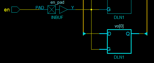
However the tool will carry on and write out a netlist containing latches, as the particular Actel device used (a ProASIC3 A3P250) contains latches as a built-in logic element. After Place and Route in Actel Designer, part of the schematic looks like this:

There are logic elements labelled DLN1, and these are latches. The letter "L" is often a clue that unexpected latches have been produced during Synthesis. You'll also see which components have been used in a report, in Actel Designer. Here is an extract:
Core Information:

    Type    | Instances    | Core tiles
    --------|--------------|-----------
    COMB    | 0            | 0
    SEQ     | 4            | 4
In this particular case, we can see that we have 4 sequential elements, even though our design can be implemented purely in combination logic - yet another clue that something has gone wrong.
Latches and Precision / Lattice
Lattice Semiconductor ispLever uses Synplify by default for synthesis, but can also be configured to use Mentor Precision RTL. To get a good variety of examples on this page, ispLever was configured to use Precision RTL, which resulted in the following message during synthesis:
Info: [45205]: "reverser.vhd", line 14: Module
  work.reverser(RTL){generic map (nbits => 4)}, Net(s) vo[3:0]: Latch inferred.
This is an interesting message as it is not even a warning - just "Info". This carries on to place and route, where there is no indication that latches have been inferred other than the list of registers (we don't expect any registers with this design).
Design Summary
   Number of registers:    4
      PFU registers:    4
      PIO registers:    0
   Number of SLICEs:             2 out of  5120 (0%)
      SLICEs(logic/ROM):         2 out of  3840 (0%)
      SLICEs(logic/ROM/RAM):     0 out of  1280 (0%)
          As RAM:            0
          As Logic/ROM:      0
   Number of logic LUT4s:       0
   Number of distributed RAM:   0 (0 LUT4s)
   Number of ripple logic:      0 (0 LUT4s)
   Number of shift registers:   0
   Total number of LUT4s:       0
   Number of external PIOs: 9 out of 147 (6%)
   Number of PIO IDDR/ODDR:     0
   Number of PIO FIXEDDELAY:    0
   Number of 3-state buffers:   0
   Number of DQSDLLs:  0 out of 2 (0%)
   Number of PLLs:  0 out of 4 (0%)
   Number of block RAMs:  0 out of 30 (0%)
   Number of GSRs:  0 out of 1 (0%)
   JTAG used :      No
   Readback used :  No
   Oscillator used :  No
   Startup used :   No
So here is an example where accidentally inferred latches results in no warnings at all.
Latches and Xilinx XST
Finally let us put the same design through Xilinx XST. The synthesis tool warns us that we have produced latches:
WARNING:Xst:737 - Found 1-bit latch for signal . Latches may be generated
  from incomplete case or if statements. We do not recommend the use of
  latches in FPGA/CPLD designs, as they may lead to timing problems.
and in the map report, we see the following:
Design Summary
--------------
Number of errors:      0
Number of warnings:    0
Logic Utilization:
Logic Distribution:
    Number of Slices containing only related logic:       0 out of       0   0%
    Number of Slices containing unrelated logic:          0 out of       0   0%
      *See NOTES below for an explanation of the effects of unrelated logic.
  Number of bonded IOBs:                  9 out of     232    3%
    IOB Latches:                          4
  Number of BUFGMUXs:                     1 out of      24    4%
Notice especially that the latches have become embedded in the pads (Input Output Block, or IOB). But we can clearly see that latches are present in the design summary.
Latches - the conclusion
- Latches are generally "a bad thing" - unless you really know what you are doing
- In synthesis, latches are not an error - they will be reported as either information or warning
- In mapping and place and route, you will not get any warnings - the mapping and place and route tools just do what the synthesis tool tells them to do!
- But you can often spot latches in the place and route summary, either as elements containing strings such as LD or DL; or explicitly listed as latches


